Main Page: Difference between revisions
No edit summary |
No edit summary |
||
| Line 1: | Line 1: | ||
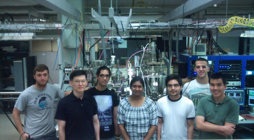
[[File:group.jpg|frame|center]] | [[File:group.jpg|frame|center]] | ||
Our group's specialty is growth and transport study of thin films grown by Molecular Beam Epitaxy (MBE) | Our group's specialty is growth and transport study of thin films grown by Molecular Beam Epitaxy (MBE). Our custom-designed MBE system has a number of unique capabilities that facilitate atomic-scale engineering of a variety of novel material systems. Utilizing these unique capabilities, we are actively investigating topological insulators, complex oxides and their heterostructures. Such heterostructures could yield new physics and devices that are intriguing both intellectually and technologically. We are currently one of the leading groups in thin film topological insulators. | ||
Revision as of 15:35, 6 October 2012
Our group's specialty is growth and transport study of thin films grown by Molecular Beam Epitaxy (MBE). Our custom-designed MBE system has a number of unique capabilities that facilitate atomic-scale engineering of a variety of novel material systems. Utilizing these unique capabilities, we are actively investigating topological insulators, complex oxides and their heterostructures. Such heterostructures could yield new physics and devices that are intriguing both intellectually and technologically. We are currently one of the leading groups in thin film topological insulators.
Job Opening
We are looking for a postdoc candidate, who will lead our new effort along oxide topological insulators. A successful candidate will be someone who is experienced in some of the following areas:
1. Thin film growth techniques: (complex-)oxide MBE, compound-semioconductor (III-V, II-VI, etc) MBE, or other thin film growth techniques adapted to heterostructure engineering of complex oxides or compound semiconductors.
2. Thin film characterization schemes: XRD, AFM, etc.
3. (Magneto-) Transport studies of thin film structures and devices (oxides, semiconductors, graphene-like materials, or topological insulators).
4. Cryogenics (sub-liquid-helium temperatures) and transport-instrumentation (+ Labview programming).
5. Photo(ebeam) lithography.
6. Paper writing skills.
Considering that many renowned groups around the world are currently working on our unique thin film structures, this position will provide additional opportunities to form strong networks with those great scientists, which will be invaluable for his/her future career.
We are planning to fill this position by early 2013.
If you are highly motivated and interested in exploring this newly emerging field, please send your detailed CV including names of three reference writers, and a research statement to ohsean@physics.rutgers.edu.
