Facilities: Difference between revisions
Jump to navigation
Jump to search
No edit summary |
|||
| (3 intermediate revisions by the same user not shown) | |||
| Line 1: | Line 1: | ||
== Growth == | == Growth == | ||
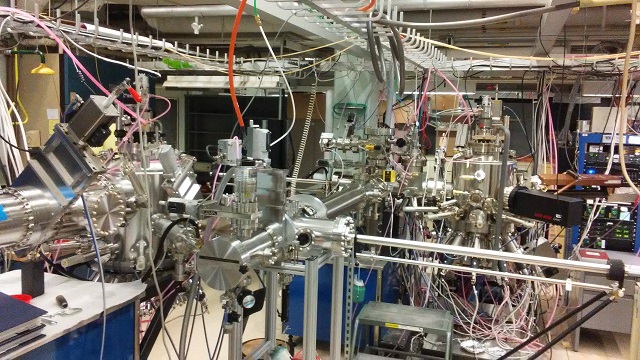
[[File:MBE-2017-2.jpg|frame|center|Our advanced Molecular Beam Epitaxy system capable of growing materials with atomic layer precision. Using this setup we can achieve epitaxial growth of complex oxides, topological insulators, and other novel materials.]] | [[File:MBE-2017-2.jpg|frame|center|Our advanced hybrid Molecular Beam Epitaxy system capable of growing materials with atomic layer precision. Using this setup we can achieve epitaxial growth of various quantum hybrid structures including complex oxides, topological insulators, and other novel materials.]] | ||
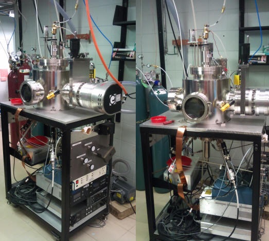
[[File:ion.jpg|frame|center| | [[File:ion.jpg|frame|center|Our lab is also equipped with a custom built sputtering/ion-milling chamber. It provides variable temperature ion milling and DC/RF sputtering capabilities.]] | ||
== Characterization & Fabrication == | == Characterization & Fabrication == | ||
| Line 10: | Line 10: | ||
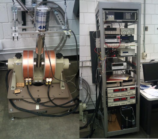
[[File:emagnet2.jpg|frame|center|Electromagnet]] | [[File:emagnet2.jpg|frame|center|Electromagnet]] | ||
[[File:AFM.jpg|frame|center|Atomic Force Microscope capable of standard AFM, Conducting AFM, Piezo-Force microscopy, Kelvin-probe microscopy]] | |||
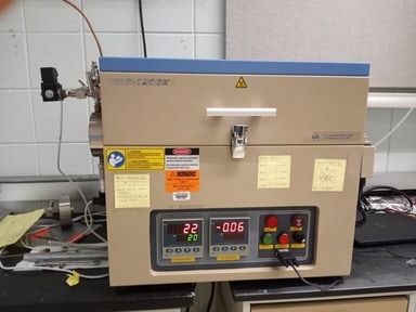
[[File:furnace1.jpg|frame|center|High Pressure Oxygen/Argon Furnace]] | |||
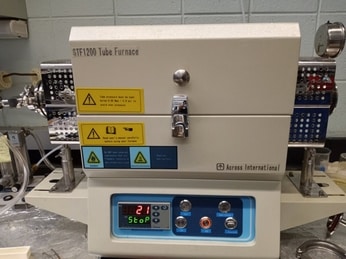
[[File:furnace3.jpg|frame|center|Oxygen/Hydrogen Furnace]] | |||
| Line 18: | Line 27: | ||
[[File:Img14.jpg|frame|center|Optical & E-beam Lithography systems | [[File:Img14.jpg|frame|center|Optical & E-beam Lithography systems for fabricating nano/micro-scale devices]] | ||
[[File:img3.jpg|frame|center| | [[File:img3.jpg|frame|center|Thermal Evaporator, E-beam Evaporator, and Sputtering chamber for device fabrication]] | ||
Latest revision as of 15:40, 20 May 2022
Growth

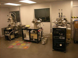
Our advanced hybrid Molecular Beam Epitaxy system capable of growing materials with atomic layer precision. Using this setup we can achieve epitaxial growth of various quantum hybrid structures including complex oxides, topological insulators, and other novel materials.

Our lab is also equipped with a custom built sputtering/ion-milling chamber. It provides variable temperature ion milling and DC/RF sputtering capabilities.
Characterization & Fabrication

Superconducting Magnet

Electromagnet

Atomic Force Microscope capable of standard AFM, Conducting AFM, Piezo-Force microscopy, Kelvin-probe microscopy

High Pressure Oxygen/Argon Furnace

Oxygen/Hydrogen Furnace

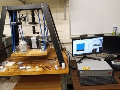
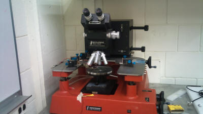
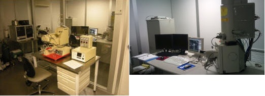
Micro-Probe Station

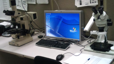
Optical Microscopy Station

Optical & E-beam Lithography systems for fabricating nano/micro-scale devices

Thermal Evaporator, E-beam Evaporator, and Sputtering chamber for device fabrication